At some time at the beginning of the design process, during development process of complex systems, we must put together a proper optical design. Usually, it is when we have already begun our system development process so we know our way around the technical details of the system. However, we have not as yet finalized the fine details of our different technical budgets. Naturally we turn to our optical designer or physicist with a set of optical requirements, give him/her a sense of direction where our Bill Of Material (BOM) budget is and then wait patiently for initial optical design concepts to choose from.
If we follow the design process to the letter we would have a concept review followed by a concept design, technical negotiations with adjacent disciplines (Optics & Physics have the most interaction with Mechanics, Control, Integration \ Manufacturing, System Engineering and in the ideal case Algo) and finally a Critical Design Review (CDR) for parts manufacturing and assembly.
You may wonder why I have chosen to concentrate over the relationship between the optical design and the Algo. As in a lot of other topics in this blog, I try to cover the pitfalls and gaps in the development process that might affect the final product’s performance. I have noticed that in many cases the interfaces with the optical designer are limited to the Mechanics, so everything will fit physically inside the product, and to the System Engineering as the project’s technical representative to ensure the optics performance. In the case where the system engineer’s knowledge of the proposed algorithms to be used in the system is not sufficiently profound, we create a gap of knowledge where the optical designer will plan what we asked for but not what we wanted or needed (and yes, I know it is a quote from the Smurfs movie).
At this particular point, a good optical designer would have and should have asked the system engineer: “what does your system do and how do you plan to do it?” (my experience in my early days was that most of the optical designers I had worked with did indeed ask these questions but only to a point). The system engineer will be able to tell a lot, but not all, as clearly stated in a previous post. If the system engineer with respect to not being the top knowledgeable man in the field of the image or signal processing algorithms used in the proposed optical system, there should be at least one meeting explaining these details to the optical designer. This is a crucial point in the design phase where gaps in the understanding of the details of any of the technical disciplines may be translated to a gap later in the project and that fixing it would be painful, both timeline and monetary budget wise.
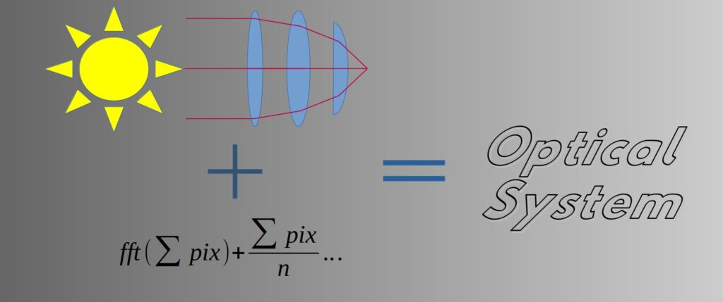
Optics and Algo go hand-in-hand
As in my other posts, I will as usual take a simple optical system example and analyze it. For the sake of simplicity, in this example we will assume that our light source is the sun, so as to avoid 2 optical devices’ alignment and illumination concept and alternative choice process. I will cover illumination design and practices in another post.
For our example we take a vision system to identify defects in fabrics in visible light. The fabric runs on a conveyor in a very fast velocity of 250mm/s. A typical defect width may be as small as 100um, and the conveyor fabric run may deviate +/-0.5mm on the focus axis.
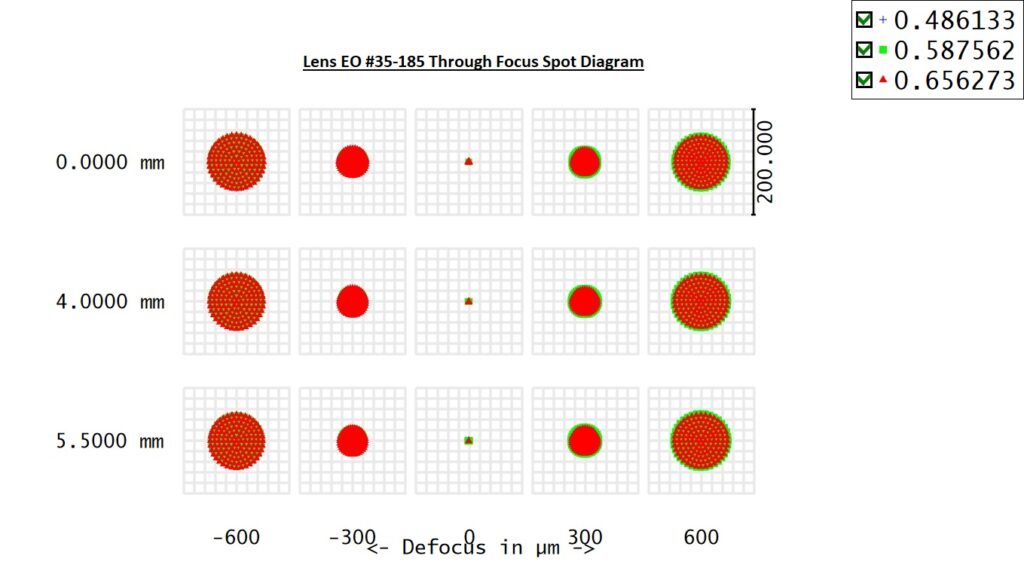
We have requested our optical designer to come up with a suitable lens + camera to cover our needs. Let’s take this off-the-shelf lens by Edmund Optics for our first example.
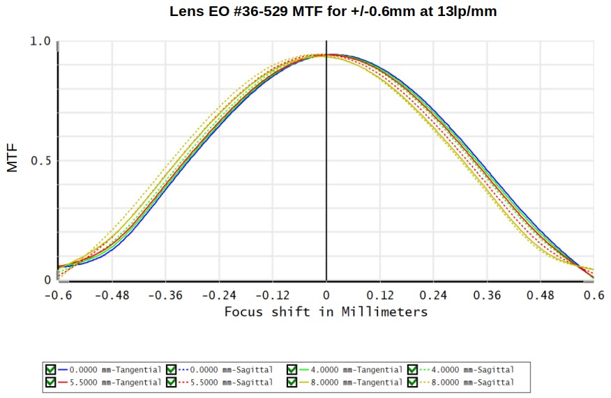
As optical designers we will take a little bit of spares so we could look at the Modulation Transfer Function (MTF) of the lens at best focus +/-0.6mm for 13lp/mm which is equivalent to ~40um line size resolution on the sample. I promise to have a dedicated post of what exactly MTF and resolution are.
The MTF graph as simulated in Ansys Opticstudio is as follows:
If we chose any camera with a 3.45um pixel size we get an effective pixel size of ~22um/pix, and because it is a conveyor running, we would recommend using a linescan color camera.
Great, thank you. We’re done! But are we really done?
First, let’s assume that our defect identification algorithm in one of its steps uses some kind of a filter with kernel size of 7X7pix. Obviously, such an algorithm cannot be easily applied to a linescan camera output, so let’s cross off the linescan camera and apply an area camera.
Next, looking at the graph above we see that around the edges of the Depth of Field (DOF) our MTF goes below 10%, however if our algorithm includes a threshold, dynamic or static, that requires numerically a greater contrast, it eliminates the edges of the DOF defect identification capabilities.
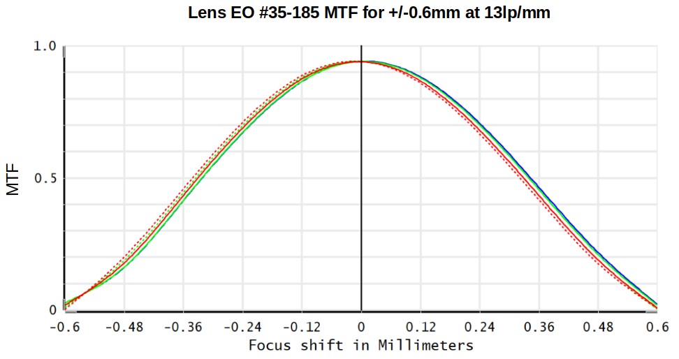
Another point to consider is the color. If we look at the following graph, we could see that the lens has some very minor, almost negligible, color aberrations.
If the base of all of our algorithms is grey-scale we should not use a color camera at all. Furthermore, as we set our light source as sun light a possible solution to eliminate the color aberrations would be to add a narrow band optical filter over the collection lens.
And last but not least, the lens costs. Let’s assume that our HW and algo may be utilized only on images up to 5Mpix at 3.45um/pix, the lens we have been exploring until now may be an overkill. If we take a look at this lens by Edmund Optics we get a significantly cheaper lens with comparable performance for our needs.
Note I did not indicate “better” or “worse” – better performance of any element or sub-module is a matter of requirements. We could have two models of the same product, in which the only difference between them would probably be different cameras, one with the first lens and the other with the second lens.
There are many more inputs from algo that may impact the optical design and vice versa. I chose only a handful as examples which could have been deducted from a few simple analysis graphs. For example, I have not taken the conveyor velocity into account, which would limit the minimum amount of light coming into the sensor and may impact our minimum contrast for the algo; or the exposure time and method (rolling shutter vs. global shutter) and how it changes the requirements from the anti-smearing algorithm and many more aspects that would have an impact.
To sum up, though this is a short post it gives a tiny taste that illustrates, through a realistic example, of how important it is to design the optics of a system hand-in-hand with its algorithm design and development. In an optical system, there are no optics without algo and no algo without optics. They are a part and parcel of the same and should be treated systematically as one even, if in practice, they are divided between two disciplines.
Getting the optical engineers involved with the planned algo at the very beginning of the design phase is the important takeaway you should have after reading this post.